This article was published in Danish, in the Danish radio armature magazine "OZ" in December 2008
|
|
600W 50MHz Dual PA,
Or, ”Waiting for sunspots”.
By Thomas Gosvig OZ1JTE.
|
|
|
The motivation.
For some time I had been looking at 4 big HF output transistors laying in my drawer at my workshop, and earlier I had got some good results building a 400-Watts 6m PA using this transistors, a TH430 (or SD1728) type, so I decided to build a dual PA. The idea was to combine 2 PA modules into a single high power system, which should be able to produce 600 Watt on 50MHz.
When the time for this idea didn’t offered many sunspots or activity on 6m, I found it to be a good time for optimize my station, instead of listing to background noise on the band every day.
Earlier the year for this project I was lucky to get a very big PA for the HF bands, so the 100 Watt from my transceiver, didn’t feel very powerful anymore.
The Seek.
I was seeking the Internet, trying to find a dependable construction, but because I want to do it “solid state”, the choices were reduced to only a few. I think that many armatures are still very nervous for using semiconductors when building high power amplifiers.
I didn’t found anything on the net, and because I needed a construction I had confidence in, I decided to make everything myself.
What I was looking for in the first place, was a push-pull construction for 48V, with included some PTT sequencer control, PA modules, filters, and then some fault shutdown of course, so I could feel pretty sure that suddenly the PA transistors wouldn’t leave the construction without permission…J
The goal was to amplify my 100Watt from my transceiver, up to about 600 Watt of output.
If I was really lucky I hoped to find a project that included PCB drawing etc.
I found out that these wishes was not to be found anywhere (not for me), and if I decided to make a project like this myself, I also had a good opportunity to make some “payback” for all the fine stuff I had found on the Internet through the years.
Parts and Boards.
I decided to make the amplifier in several smaller boards. I could then easily make something new or make adjustments, if I needed something else.
I had never before made anything else then handmade drawings of schematics etc., but I realized that this project needed to have something to control my work on a better way.
I had to try out some of the good PCB and Schematic software, that could be found on the Internet.
My choice was DesignWorks ekspress (Reference 1) for the schematic part, and ExpressPCB (Ref:2) for the PCB part.
Despite I only very limited had used this type of software before, I quickly got a nice feeling working with these two fine pieces of free software.
I can only recommend this software, for projects like this, and for an inexpert like myself.
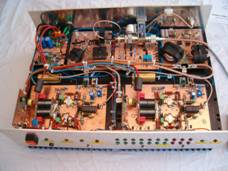
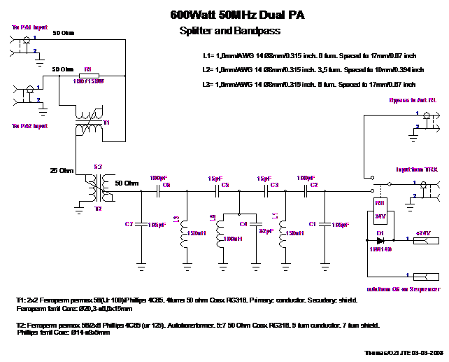
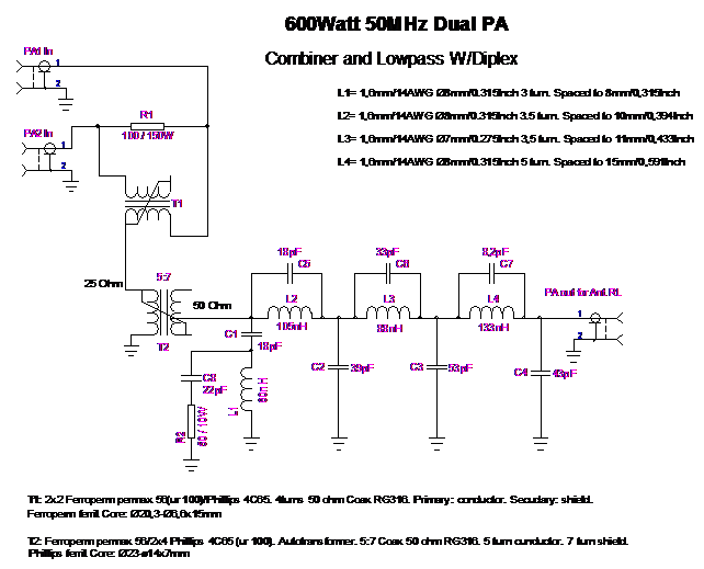
The main parts of this project is the power supply, input splitter and filter/relay board, the two major PA-modules, witch easily produce 300Watt each from the 2x250Watt transistors, and then the signal pass through a SWR bridge, a power combiner and lowpass filter board, and then the clean 50Mhz signal at 600 Watts meet a coax relay, just before the antenna socket.
The internal wiring can be seen in the block diagram.|
|
|
|
|
|
Controller unit |
Bandpass unit |
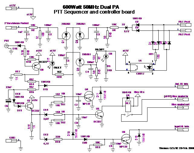
Protection and Controls.
When you are building a solid state PA amplifier like this one, there is something in the design you just can’t ignore.
Look at (Ref: 3) for ”What makes a good solid state amp”.
Timing of the relay switchover, and the ability to make a very fast shutdown if something goes wrong, is extremely important issues for reliable performance of the amplifier.
ALC loops and other fault protection circuits must have the right timing.
Some typical issues you meet in broken PA amplifies are high VSWR, too much output, and open antenna relays.
All these issues can cause second breakdown (Litt 4) in the PA transistor, which are one of the most frequent reasons for PA transistor death.
Besides the problems above, heat, overvoltage, oscillation etc., are things you need to be aware of in the design.
To monitor the kind of faults, I have estimated to be the most risky ones, I made a couple of protection circuits. These protection signals are connected to a controller board. This board will evaluate the signals and will start a “shut-down” sequence if something goes wrong.
I have made protection for “Second breakdown”, “High SWR”, “To High output”, and in a attempt to avoid high IMD, and to protect the other PA module, if one PA module should fail, I also monitor the difference in output from the 2 PA modules.
Furthermore on this controller board, I also have a sequencer for the PTT control, which control the timing of the input relay, the bias keying, and the antenna relay. This timing will be controlled in both the “normal state” and also in a “shut-down” sequence.
I know all this would be an easy job for a PIC to control, but I felt more confident to do it in the old fashion way..J.
|
|
|
|
|
|
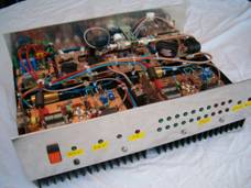
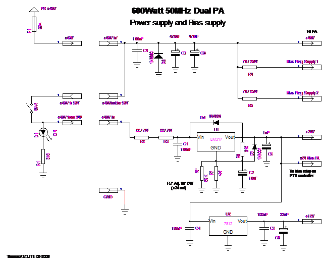
Power supply |
Combiner, Lowpass and coaxrelay |
Circuit boards.
I don’t believe that this project is a typically beginner project, and I have chosen not to explain every little detail in the schematics. I think that most of the people, who want to use this article to build their own amplifier or try to duplicate this PA, would already have a good understanding about the details.
I also have damped the theoretical part, because I very easily could find a lot of theoretical articles on the Internet myself, but what I really missed was an article which showed me a kind of practical “I have made it this way”.
Instead I will try to focus on the part where I had the biggest concern.
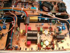
I can’t find much to say about the power supply. This board make +12V and also +24V out of the +48V input.
+24 V is made by a LM317T I have chosen because of the high voltage between the input and output terminals. +12 is made by a normal 7812 voltage regulator unit.
|
|
The 50Mhz input signal passes the input relay and meet a band pass filter, which are designed just to cover 50-52MHz. The 3db points are at about 43 and 55MHz, and because the filter is pretty narrow, then the insertion loss is about 1db.
I didn’t emphasised the insertion loss very much, because I felt that I would have plenty of gain in my transistors to compensate for this loss, and I felt it was more important to clean up the signal from the exciter. Only a little “hiccup” from an unclean exciter will be risky because of the high gain in the transistors, and the lack of low frequency feedback in this design.
After the band pass filter the signal meet the signal splitter, and I think this unit is one of the components that give most people great concerns.
|
|
When I was working on my design I considered many types of signal splitter/combiners.
I chose a broadband transmission line type, made on some ferrite toroids that would handle the power and frequency. The permeability should be around 100.
This transmission line type has low insertion loss, is broadbanded, and is not critical in the way you make it.
You can have a further look into this subject in an article by Joergen OZ7TA in the Danish OZ magazine from1990 (Ref:5). The article is in Danish language.
Maybe it will be easier to understand the splitter component in the combiner function.
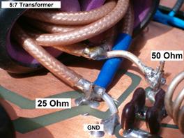
Here you have two 50 ohm signals, that goes via a balun transformer and end up as one 25 ohm signal. After this the signal meet another transformer, which will transform the 25 ohm to 50 ohm in a 1:2 transformation.|
|
The splitter is exactly the same unit as the combiner, but just the other way around.
Also a autotransformer, which transform the 50 ohm to 25 ohm, and then a balun. The balun split the one 25 ohm signal into two separate 50 ohms signals.
The way you have to wound this transformer can be a little had to describe, so I hope you will catch the idea from the pictures, and the text from the schematic.
It will be significant that the cable lengths, to and from all the ports, are exactly the same.
This will insure that the 2 PA modules work exactly on the same point on the signal curve.
When I measured the signal splitter, using my miniVNA, the fault in phase was below 1 degree, and the insertion loss was 3.2 db for each port.
The complete insertion loss from the relay, signal splitter and band pass filter was about 4.2 db for each port. Remember that the first 3 db will occur just when splitting the signal in two.
Now I will explain a little about the high insertion loss in the band pass filter.
It was important for me to protect the amplifier in any way I could, so I decided to design it for 100W input, so I didn’t one day forgot to turn my power down on the transceiver, and because of this was overdriving the amplifier.
The high insertion loss was then also an “input attenuator”
Later on I realized that I could very well had used 0.5db more gain in the complete PA.
|
|
|
|
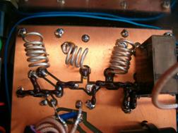
Detailes 5:7(1:2) transformer |
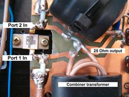
Detailes Combiner transformer |
More important was the insertion loss in the lowpass filter and the power combiner.
The insertion loss for the low pass was 0.22db and for the power combiner the insertion loss was 0.11db.
Not extremely accurate measurements, but it seems to be satisfying.
The Balun transformer is wound on Permax 56 ferrite from Ferroperm, and the 5:7(1:2) transformer is wound on Phillips 4C65 toroides. As you can see in the part list I had to glue 4-6 toroides together to reach the needed amount of ferrite
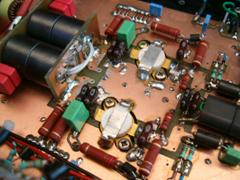
PA modules.
The PA module is of course the main part and the heart of this project.
My goal was to amplify my 100 Watt up to 600 Watt.
When splitting the 100 Watt signal into 4 equal transistors, as here into 2x2 in this push-pull system,I had about 20 Watt for each transistor.
This power level should be enough drive for each device to obtain the wanted output.
The datasheet (Ref:6) for the TH430 or SD1728 device showed a gain between 14.5 and 10db when using the device between 30 and 70Mhz.
I quickly realized that “Datasheet single frequency gain” is not the same as “homebrew broadband design” gain.
Do not expect any more then 8-10db gain.
|
|
Although the main idea in this project was to optimize everything for 50MHz, you can very well change the frequency to another band, because none of the filters is a part of the PA module board.
When I tested one of the first prototypes of the PA without any low frequency compensation, I had no problems to obtain about 120W out of the system with only 2.5 watt of input on 20m. This is 17 db gain at 14Mhz, so I quickly realized I had to make some kind of low frequency compensation, so the system wasn’t to hysteric on low frequencies. The gain would go further up on 80 and even 160m, but I didn’t’ dared to check out the gain on these bands.
This is why I designed the narrow bandpass filter.
Another low frequency compensation is R9/R8 together with C12/C13. These values have most impact at low frequencies, and not much at 50Mhz, because of the ferrite bread in the feedback.
Also the RF choke in the bias supply has a little optimizing on 50Mhz. The normal 3½ turns is optimized to only 1½ turn. Still sitting at the 6- hole ferrite core.
Anything else is pretty straight forward, and uses normal HF technique.
I learned a lot of the basics PA technique when I studied a Danish article from Joergen OZ7TA published in the Danish OZ magazine back in 1990. (Ref:7).
I also made a more basic PA article myself, in the same magazine back in 2007 (Litt 8).
(Also here the language is Danish).
But some of the technique I have used in this PA is new.
Lot of things are done to prevent failure on the pressures TH430 devices, and because of this I have also implemented some special circuits.
The second breakdown fault I described above can be avoided if you monitor the voltage at the TH430 collector, and seek to shut down, or adjust the input to a lower level, if the collector voltage rises to a dangerous high level.
I don’t think many people like to use 4 oscilloscope probes at one time, to measure the voltage on each collector, and that is why I have 4 built-in RF probes that monitor this voltage, and tell the controller board when to shut down.
We just could remove the bias supply and change the overall gain, but we don’t want to take any chances at this point, so I let the amplifier shut down completely. (Disable the PTT).
The R1 value on the controller board will decide when to close down. I have chosen a value about 96V, but this value is pretty conservative, and has good headroom up to the limit at 110V.
If you are gutsy you can step a little more on the accelerator.
At 96V the signal start to be shunted internally on the PA module via a 22 ohm resistor.
|
|
|
|
Detailes PA Module |
Detailes PA Module |
 |
|
|
|
|
|
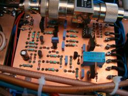
SWR bridge |
Output transformer |
Rear panel |
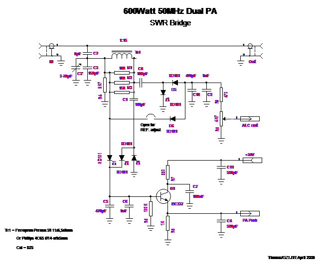
SWR Bridge.
This unit is well known by most Hams.
The 2 little units right behind the PA modules will detect high SWR but also peak power from each of the 2 PA modules.
The trained eye will notice that this kind of transformer is not the normal transformer used in this kind of SWR Bridges.
This transformer has no center tap, and both the reflected and the forward voltage will be combined into one voltage that will tell us about the load of the PA unit..
The two peak output from each unit is wired to the controller unit, where these two signals will be evaluated. D1 on the controller unit will determine when to shut down.
Because we already have these two signals on the controller unit, we also use them to detect any difference in the two signals. This is done by U1. U1 will then determine when to shut down because of the difference in output from the two PA modules.
The SWR Bridge also has a negative going voltage detector, used for the ALC control of the transceiver.
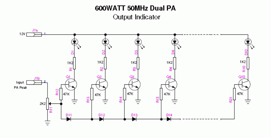
Output indikator.
This unit is a little ”extra gadget”, and will give a little life in the shack, when you are shouting in your microphone.
VU meters that just will show you “It’s alive”.
I haven’t made any printed circuit board for this unit, but it is very simple to make on a little piece of experimental pcb board.
 |
The Construction.
As described earlier I made my pcb’s using real pcb software, and maybe because of this, my first real attempt to make this kind of boards, I unfortunately made a slip when routing the traces for the devices in TO220 package. So be very careful when mounting Q3/Q4 on the PA module, and also U1/U2 at the power supply. It will need your full attention.
I put my U1 and U2 underneath the pcb, and then it will fit correctly to the solder points.
I have used 2 separate heatsinks, each 22x29cm, composed to one big surface. This big brick is also the bottom of my chassis.
Everything is made from double sided circuit boards, and one of the sides is always a full unetched copper surface.
Be aware of one single connection you have to do yourself. You need a wire from the 2 rectifier bunch D5-12 and D13-20. You can make this cathode to cathode connection with a little piece of Teflon (PTFE) coax cable underneath the pcb.
Always remember to make a lot of plate through holes to insure good RF grounding everywhere.
This is especially important at the PA modules, and near the TH430 devices.
I have turned some of the boards upside down, so I more easily could make some changes in the design if needed.
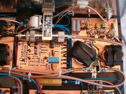
I hope most of the details will be clear when looking at my pictures.
Also remember to ground the flange (bottom) of the output transistors with a little “I don’t know what you call it solder gadget”, and also make a little roof of tin plate on top of the transistor package.
The results.
The PA modules I have described above will easily deliver 300 Watt each, but the gain became not as high as I expected. I hoped for minimum 9db, but I only got 8.5db.
When the loss in the input filter also are a part of the calculation, then we only have (8.5db-1.1db) 7.4db left. Then the 100 Watt from the transceiver will end up as 525 Watt. Not quite 600 Watt.
If the input bandpass filter was designed to only 0.5db of loss, then the calculation will end up with an output of 600 Watt.
From here I had 2 options. To design a new input bandpass filter (see Ref: 9 for an easy solution) and slack a bit on the protection circuits, or to stop at this level and be happy with my results
My 4 ele. HB9CV antenna was only rated for 400 Watt, so I decided to stop at this point.
Of cause I one day will make another filter, but for now I am satisfied.
The complete unit draw just about 20A (57% affectivity), so you need a big solid 48V supply when you fire this baby up.
I am pretty sure that you can drive this unit up to even more output, but you have to be fearless and very careful.
Maybe a 1:3 output transformer and a small modification in the protection circuit will do the trick.
And then of cause you will need a little more input drive.
This amplifier is optimizes for 50Mhz, but because of the classic HF technique used, it could easily be changed for other HF bands.
With a little attention at the low frequencies compensation in feedback and output transformer and ferrite, then this design should work from 1.8 to 30Mhz as well. Maybe 1.8-50Mhz with a little lower gain at 50Mhz could be realized.
I was lucky to get my output devices from some old and discontinued marine telephones, but if you are able to get some other type of devices you can of cause modify this design to other types of output transistors. Some new values of the capacitors close to the output transistors have to be found again if you change the output devices to some other types.
Good luck, and I would be happy to hear about your own project.
Vy 73 de Thomas/OZ1JTE
You do not have permission to copy, display, or publish these materials on another web site without prior written consent. Under no circumstances can you use or publish, in any way, any content for commercial or promotional purposes or claim the material as your own.
Cross reference:
1. http://www.capilano.com/ DesignWorks Express
2. http://www.expresspcb.com/ Express PCB
3. http://www.ab4oj.com/quadra/sshfamp.html What makes a good solid state amp.
4. http://www.keithley.com/data?asset=5186 Second breakdown
5. OZ7TA Jørgens “En 0 graders to port powersplitter/combiner “OZ” April, 1990.
6. http://www.datasheetcatalog.org/datasheet/stmicroelectronics/2889.pdf
7. OZ7TA Jørgens “Bredbånds HF PA-trin med transistorer” “OZ” Temahæfte 1990.
8. OZ1JTE Thomas ”QRP Booster” ”OZ” April 2007.
9. http://yu1lm.qrpradio.com/6m%20BP%20FILTER-YU1LM.pdf